 Semiconductor
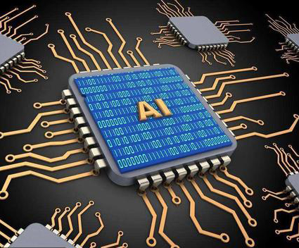
 With the rapid development of science and technology, smart home, artificial intelligence, automatic driving, 5g, battery energy storage and other high technologies have entered the lives of ordinary people, which benefits from the continuous innovation and development of the integrated circuit industry. Integrated circuit, also known as IC, refers to the production of specific functional circuits on the wafer through a special semiconductor process flow. It follows Moore's law and goes on from generation to generation. Nowadays, there are hundreds of millions of transistors on an integrated chip the size of a fingernail.
The fabrication of chip mainly depends on micro machining, automation and chemical synthesis technology. The whole process includes: chip design, wafer manufacturing, testing, packaging and so on, among which wafer manufacturing is the most complex process so far. The wafer manufacturing process includes ion implantation, wafer testing and chip testing, which are all inseparable from refractory metal materials.
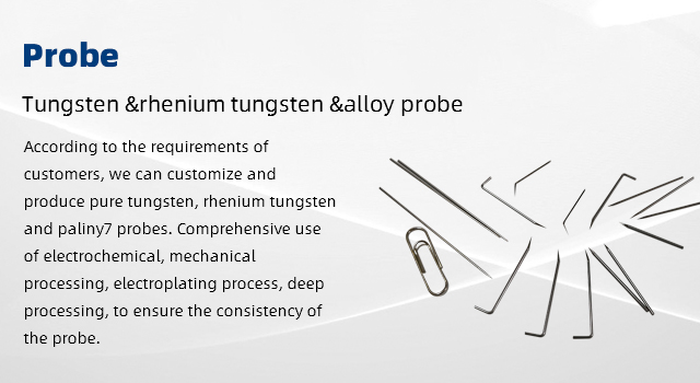
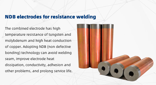
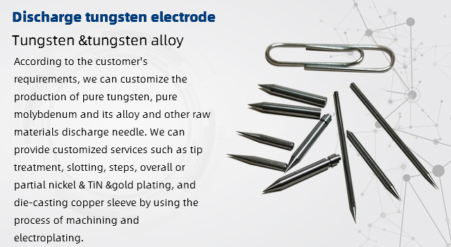
Our high temperature components made of tungsten, molybdenum and tantalum are used in the ion implantation process. Due to their excellent corrosion resistance, high strength, high thermal conductivity and other characteristics, they ensure the efficient generation of ions. On the optical path to the wafer, the ions are accurately guided and free of impurities. Chip testing technology belongs to the key field of semiconductor industry. We use probes made of pure tungsten, tungsten rhenium, paliney 7 and other raw materials, which are suitable for all kinds of pad surfaces, among which tungsten, tungsten rhenium probes have the characteristics of high purity, high hardness, high modulus of elasticity and so on. Hengmi probe has been used in IC, wafer, led detection and scientific research fields.